May 11, 2026
· 13 min readWhy Google Built Two AI Chips Instead of One — Inside the TPU v8 Split
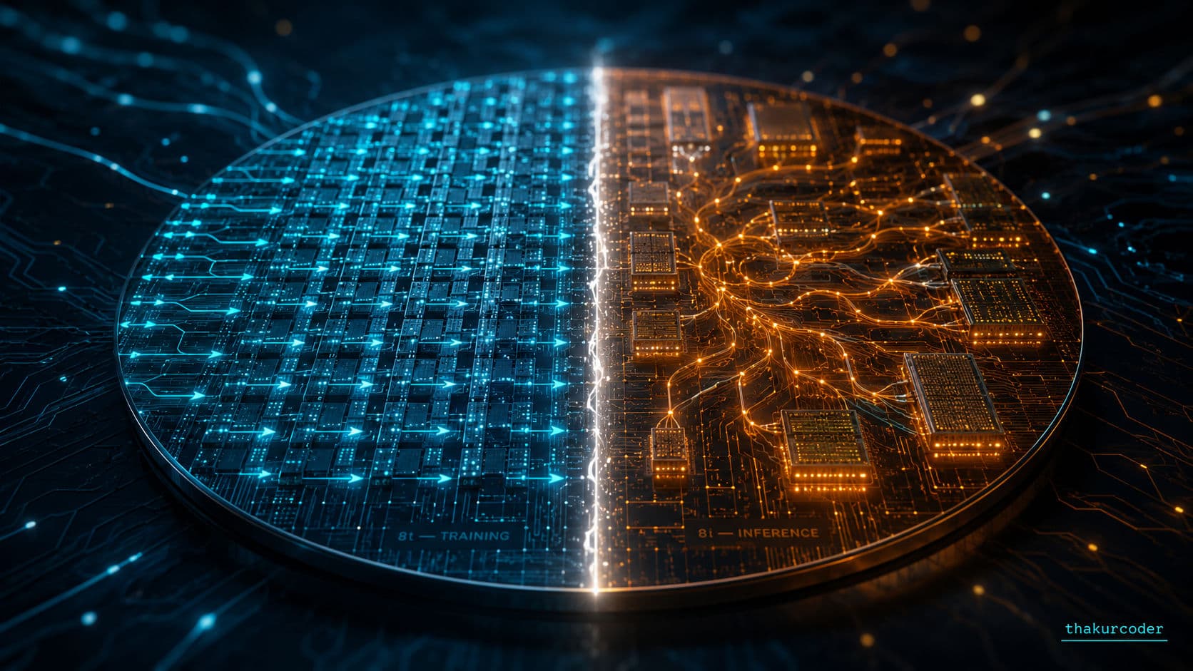
Google's eighth-generation TPU isn't a chip — it's two. The TPU 8t targets training, the TPU 8i targets agentic inference, and the reason for the split tells you where AI hardware is heading. This post builds the story from the silicon up: how CPUs, GPUs, and TPUs actually differ, what a systolic array does, and why one chip can no longer be optimal for both halves of the AI workload.
TL;DR
- Google's eighth-generation TPU ships as two chips, not one: TPU 8t for training, TPU 8i for inference.
- Training is compute-bound (raw FLOPs, interconnect bandwidth). Inference is memory-bound (KV cache, single-token latency). One chip can't be optimal for both.
- TPU 8t scales to 9,600 chips per superpod with 121 exaflops of FP4 compute. TPU 8i scales to 1,152 chips per pod with 384MB of on-chip SRAM to hold the KV cache.
- Both run on Google's in-house Axion ARM CPU host — first time Google has gone full-stack accelerator + CPU.
- Up to 2x performance per watt vs the previous Ironwood TPU.
- The architectural signal matters more than the specs: AI workloads have diverged enough that specialization beats general-purpose silicon.
Why this announcement matters
Google announced its eighth generation of TPUs at Cloud Next 2026. The headline isn't the spec sheet — it's that there are two spec sheets. For the first time in the TPU program's decade-long history, Google is shipping two distinct chip designs in the same generation: TPU 8t targets large-scale model training, while TPU 8i is built for low-latency inference and reasoning workloads.
The decision predates the announcement. "We realized two years ago that one chip a year wouldn't be enough," Google's SVP Amin Vahdat said onstage — meaning the split was committed in 2024, before reasoning models and agentic inference dominated the frontier conversation.
To understand why this matters, we need to build up from the silicon. What does a CPU actually do? What does a GPU do differently? What does a TPU do that neither can? And why have AI workloads diverged enough that one chip can no longer cover both ends?
The CPU: general-purpose, expensive cores
The chip running your laptop right now is a CPU — a central processing unit. It's been the foundation of computing for fifty years. A CPU is made of cores, and a core is the smallest hardware unit that can independently fetch an instruction, decode it, execute it, and write the result back.
Every core has its own pipeline, registers, and arithmetic logic unit (ALU). It can run one thread completely on its own. When your laptop has 8 cores, that's 8 independent execution units on the same piece of silicon — your browser on one, your IDE on another, your video call on a third.
Modern CPU cores are also extremely sophisticated. They have:
- Branch prediction — guessing which way an
ifwill go before the condition is evaluated. - Out-of-order execution — reordering instructions on the fly for better throughput.
- Large caches — multi-level L1/L2/L3 to hide memory latency.
- Wide instruction sets — x86-64 has thousands of instructions.
All of which is why a CPU is general-purpose. Anything you can write, a CPU can run — operating systems, compilers, databases, games, browsers.
But each core is large, expensive, and you can only fit so many on one die. Consumer CPUs top out around 16 cores. Server CPUs reach maybe 100. That's the ceiling.
That ceiling worked fine until about a decade ago. Then AI happened.
The GPU: parallel by accident
Training a neural network isn't a complex task. It's a simple task repeated billions of times. At the heart of every neural network is one operation: matrix multiplication. Multiply a matrix of inputs by a matrix of weights, add a bias, you have one layer's output. Do this a few hundred times and you have a forward pass through a language model.
The operation is trivial — a multiply and an add. The scale is enormous. A single forward pass through Gemini or GPT involves trillions of multiply-add operations.
A CPU can do this. A CPU can do anything. But 16 cores doing trillions of operations 16 at a time would take years.
What we actually need is not 16 smart cores. You need 16,000 dumb ones. And the chip that fits that description already existed — built for video games, not neural networks.
That's the GPU — graphics processing unit. When you render a frame, every pixel needs a color computed. A 4K frame has over 8 million pixels, and most of those computations are independent. The color of pixel 1 doesn't depend on pixel 2.
So GPU designers at Nvidia and AMD made a different trade-off: thousands of small cores instead of a few big ones. A modern Nvidia H100 has over 16,000 cores. Each one is far less sophisticated than a CPU core — no branch prediction, limited instruction set, just enough hardware to do arithmetic fast.
GPUs are organized differently too. Those cores are grouped into blocks, and every core in a block runs the same instruction on different data. This model is called SIMD — Single Instruction, Multiple Data.
Around 2012, researchers noticed that matrix multiplication — the math behind neural networks — is structurally identical to the math behind graphics. Big grids of numbers multiplied and added in parallel. A perfect fit for a GPU.
That accidental match is how Nvidia went from a graphics card company to the most valuable chip company in the world. Every major AI model — GPT, Llama, Claude — is trained on GPUs.
But notice the word accidental. A GPU is still a general-purpose parallel chip. It does graphics, physics, cryptography, AI — good at all of them, optimal for none. That's the gap Google decided to close.
The TPU: built for one job
Google started building the TPU — Tensor Processing Unit — in-house around 2015. A TPU is not general-purpose. It can't run an operating system. It can't render a frame. It has one job: matrix multiplication, at maximum efficiency.
The clever part is a structure called a systolic array. Picture a 2D grid of small hardware units. Each unit can do exactly one thing — take two numbers in, multiply them, add the result to a running total, and pass the result to its neighbor.
At each clock tick, every unit multiplies its two inputs, adds the accumulated value from above, and passes everything along. A matrix multiplication that would take a GPU thousands of separate memory reads and instruction fetches happens on a TPU as one continuous wave of data flowing through the grid.
- No instruction decoding on every step.
- No fetching operands from memory on every step.
- The data just keeps moving through the chip itself.
Less time waiting, less power on control logic, more time on actual math. The trade-off is total: a TPU can't do anything else. But for matrix multiplication, it's dramatically more efficient per watt than either a CPU or a GPU.
Google has been running TPUs quietly for years. They power search ranking, YouTube recommendations, Translate, and every version of Gemini. You've been using TPUs without knowing it.
Training vs inference: two different problems
Which brings us to why Google built two chips this generation. The realization the industry has been slowly accepting: training a model and serving a model are different problems.
They look similar on paper — both are forward passes through a neural network. In practice, they stress the hardware in opposite directions.
| Dimension | Training | Inference |
|---|---|---|
| Bottleneck | Compute | Memory |
| Batch size | Massive | Often 1 (per token) |
| Pattern | One huge matrix multiply, then sync gradients | Sequential token generation, growing KV cache |
| What matters | Raw FP4/FP8 FLOPs, chip-to-chip bandwidth | On-chip SRAM, memory bandwidth, latency per hop |
| Failure mode | Slow gradient sync stalls the whole cluster | KV cache misses force expensive memory reads |
| Goal | Throughput | Latency |
Training is compute-bound. You're pushing trillions of examples through the network, running massive batch sizes, doing the same matrix multiplication billions of times. You want raw floating-point throughput and very high bandwidth between chips so they can share gradients between training steps.
Inference is memory-bound. The model doesn't process one huge batch — it generates one token at a time, back to back, waiting on memory between each step. For long conversations, the model holds a large key-value cache in memory that grows with every token generated.
Agentic inference makes this dramatically worse. An AI agent isn't one query — it's a loop of queries, calling tools, reading results, planning next steps. Every millisecond of latency compounds across the loop. In this age of AI agents, models must reason through problems, execute multi-step workflows and learn from their own actions in continuous loops. That demands hardware tuned for round-trip latency, not bulk throughput.
Once you accept these are different workloads, the split makes sense.
TPU 8t: the training powerhouse
The TPU 8t (code-named Sunfish, designed in partnership with Broadcom) is the training chip. It is built for maximum compute throughput at massive scale.
The headline numbers:
| Metric | TPU 8t |
|---|---|
| Chips per superpod | 9,600 |
| Compute (FP4) | 121 exaflops per pod (12.6 PFLOPS per chip) |
| HBM per chip | 216 GB HBM3e |
| Memory bandwidth | 6.5 TB/s per chip |
| On-chip SRAM | 128 MB |
| Scale-up bandwidth | 19.2 Tbps per chip |
| Scale-out networking | 400 Gbps per chip |
| Network topology | 3D Torus, scales to 1M+ chips via Virgo Network |
A few architectural points worth flagging:
SparseCore stays. Central to TPU 8t is the SparseCore, a specialized accelerator designed to handle the irregular memory access patterns of embedding lookups. Embedding lookups are everywhere in modern training — recommender systems, multi-modal models, retrieval — and they don't fit the dense MXU model.
Native FP4. TPU 8t introduces native 4-bit floating point (FP4) to overcome memory bandwidth bottlenecks, doubling MXU throughput while maintaining accuracy for large models even at lower-precision quantization. Fewer bits per parameter means less data movement, which is the actual bottleneck on most training runs.
Virgo Network. A new networking architecture supporting 8t clusters (Superpods) can scale beyond 1 million TPU chips in a single training job via a new interconnect Google is calling Virgo networking. A million chips in one logical training cluster is the headline benchmark Google wants you to remember.
TPUDirect Storage. Data moves from Google's managed storage tier directly into HBM without going through the host CPU. Removes a hop that gets expensive at scale.
Google claims TPU 8t delivers up to 2.7x performance per dollar over the previous Ironwood TPU for large-scale training.
TPU 8i: the inference specialist
The TPU 8i (code-named Zebrafish, designed in partnership with MediaTek) is the inference chip. Smaller pods, different priorities.
| Metric | TPU 8i |
|---|---|
| Chips per pod | 1,152 |
| Compute (FP4) | 10.1 PFLOPS per chip |
| HBM per chip | 288 GB HBM3e |
| Memory bandwidth | 8.6 TB/s per chip |
| On-chip SRAM | 384 MB (3x previous gen) |
| Scale-up bandwidth | 19.2 Tbps per chip |
| Network topology | Boardfly (reduced network diameter) |
Three things make this chip interesting:
384 MB of on-chip SRAM. SRAM is the fastest memory a chip can access — it sits right next to the cores. Tripling it lets the KV cache stay on-chip during long-context inference. According to Google, all that SRAM helps the TPU 8i keep more of the key-value cache (model's short term memory) resident on chip and reduce the amount of time the cores are left waiting for data. This is the single biggest lever for inference latency.
Collective Acceleration Engine (CAE). Replaces SparseCore on this chip. The accelerator block speeds up inference by offloading collective communications, like all-reduce or all-gather, shortening synchronization stalls that would otherwise leave the chip's tensor cores sitting idle. Google says the CAE reduces collective communication latency 5x.
Boardfly topology. A new network topology specifically designed to minimize the number of hops between any two chips in a pod. Training networks optimize for bandwidth; inference networks optimize for diameter. Boardfly is built for the latter.
Google claims TPU 8i delivers up to 80% better performance per dollar over Ironwood for large MoE inference at low-latency targets.
💡 Why MoE matters here: Mixture-of-Experts models route each token to a different subset of expert subnetworks, which may sit on different chips. Chip-to-chip communication becomes unpredictable, so low-latency collectives matter more than raw bandwidth. CAE and Boardfly are both built for this.
The Axion CPU and the full-stack story
Both TPU 8t and TPU 8i run on Google's in-house Axion ARM CPU as the host processor. "By owning the full stack, from Axion host to accelerator, we can optimize system-level energy efficiency in ways that simply cannot be achieved when the host and chip are designed independently," Vahdat said.
This is the first time Google has gone fully in-house — custom CPU plus custom accelerator, top to bottom. The result is up to 2x better performance-per-watt compared to Ironwood.
The bigger picture: specialization is winning
Step back from the specs. The bigger architectural signal is this:
Nvidia's strategy for a decade has been one chip for everything. Training, inference, scientific computing — all on the same GPU family. Sell millions of them. Let the software figure out the workload.
Google is quietly betting against that. They're saying training and inference have diverged enough that you can no longer optimize one chip for both. You either specialize or you lose on efficiency.
Google isn't alone. AWS has done this for years with Trainium and Inferentia. Nvidia has also dabbled with this kind of specialization, though not to the same extent. The GPU slinger's Blackwell Ultra generation was optimized specifically for AI inference, trading high-precision grunt for a 50 percent jump in memory and FP4 compute over its Blackwell sibling. Meta is building MTIA for inference. Microsoft is shipping Maia 200.
The market hasn't fully decided yet. Nvidia's stock barely moved on the v8 announcement. But the architectural direction is clear: purpose-built silicon for purpose-defined workloads.
What this changes for production teams
If you're running AI workloads in production, here's what TPU v8 actually changes for procurement decisions over the next 18 months:
- Training teams: Look at TPU 8t availability windows, Virgo networking access, and goodput SLAs — not just headline EFlops. The 1M-chip claim only matters if you can actually book that capacity.
- Inference and agent teams: Look at TPU 8i availability on Vertex AI, independent latency benchmarks as they emerge, and whether 288 GB HBM-per-chip fits your context window economics.
- Gemini Enterprise consumers: You'll inherit the 8i lift through the API automatically. Expect the ceiling on what you can deploy in production to rise meaningfully through 2026.
- Anyone evaluating Nvidia alternatives: TPU v8 is the first generation where the cost-per-token gap may be large enough to justify migration friction. Independent third-party benchmarks will start landing in Q3 2026.
⚠️ Caveat: General availability is still "later in 2026." All benchmarks are Google's own. Wait for independent numbers from early cloud customers before committing to architectural changes.
Conclusion
The TPU v8 split is the moment AI hardware stopped pretending one chip could do everything well. Training and inference now have different network topologies, different memory hierarchies, different accelerator blocks, and increasingly different design partners (Broadcom on training, MediaTek on inference).
For most teams shipping AI today, this changes very little in the short term — you'll keep using the API you already use. But the architectural divergence is worth tracking, because it tells you where the cost curve is heading. The teams that win on inference economics in 2027 will be the ones running on hardware where the KV cache lives in SRAM, the collectives are accelerated in silicon, and the network topology was built for latency rather than throughput.
That's not Nvidia's roadmap today. It is Google's. And the gap between the two architectures will probably define cloud AI economics for the next three years.
Cover image prompt (thakurcoder dark cinematic palette):
A high-angle, cinematic close-up of a single silicon wafer split visually into two distinct halves — left half glowing in electric cyan (
#22D3EE) representing dense, ordered training compute with subtle grid patterns of multiply-accumulate units; right half glowing in warm amber (#F59E0B) representing fluid, agentic inference paths with flowing data trails connecting smaller memory blocks. Background is deep navy (#0A1428) with faint topographic circuit traces. Dramatic side lighting, shallow depth of field, subtle bokeh from interconnect optical fibers. No text, no logos, pure concept rendering. Cinematic, premium, almost product-shot quality.
FAQ
What is the difference between TPU 8t and TPU 8i?
TPU 8t is built for training — maximum compute throughput, massive scale-up bandwidth, and 9,600-chip superpods. TPU 8i is built for inference — more on-chip SRAM, more memory bandwidth, and lower latency at smaller 1,152-chip pods. Both share a foundation but are tuned for opposite bottlenecks.
Why can't one chip be optimal for both training and inference?
Training is compute-bound and benefits from raw FLOPs and huge interconnect bandwidth. Inference is memory-bound — it generates one token at a time, dragging a growing KV cache through memory on every step. Optimizing for one workload trades off the other, so specialization wins on efficiency per watt and per dollar.
What is a systolic array and why does it matter for AI chips?
A systolic array is a 2D grid of multiply-accumulate units where data flows rhythmically between neighbors. Inputs enter from the top, weights from the side, and each unit multiplies, accumulates, and passes results on every clock cycle. It turns matrix multiplication into one continuous wave instead of millions of separate memory and instruction fetches.
How does a TPU differ from a GPU?
A GPU is a general-purpose parallel chip with thousands of small cores, originally built for graphics and adopted for AI because matrix math fits SIMD execution. A TPU is purpose-built for matrix multiplication via systolic arrays, with no general-purpose instruction set. The TPU trades flexibility for far better efficiency per watt on the specific workload it was designed for.
Will Nvidia's one-chip-fits-all strategy still work?
Nvidia has hinted at specialization too — Blackwell Ultra is tuned for inference — but its core strategy is still a unified GPU line. Google's bet is that training and inference have diverged enough that you can no longer optimize one design for both. The market hasn't decided yet, but the signal is strong: AWS, Google, and Microsoft are all building inference-specific accelerators.
When will TPU v8 chips be available?
Both TPU 8t and TPU 8i are scheduled for general availability later in 2026 through Google Cloud's AI Hypercomputer platform. Anthropic is the anchor customer with a 3.5 GW capacity commitment starting in 2027.